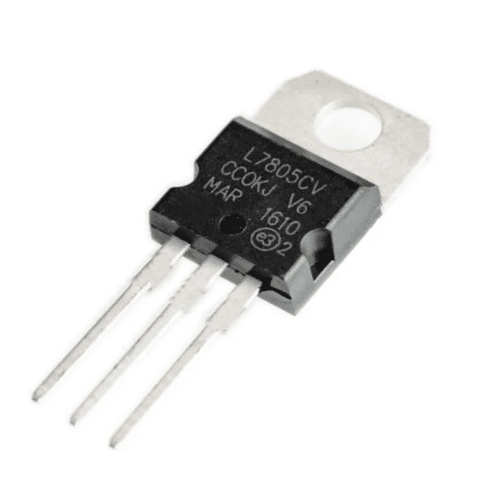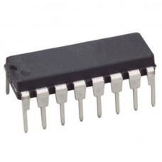
CD4504 - Hex Voltage Level Shifter IC
CD4504 - Hex Voltage-Level Shifter IC
The CD4504 hex voltage level shifter IC consists of six circuits that shift input signals from the VCC logic level to the VDD logic level. To shift TTL signals to CMOS logic levels, the SELECT input is at the VCC HIGH logic state. When the SELECT input is in a LOW logic state, each circuit translates signals from one CMOS level to another.
The CD4504 types are supplied in 16-lead hermetic dual-in-line ceramic packages (F3A suffix), 16-lead dual-in-line plastic packages (E suffix), 16-lead small-outline packages (M, M96, and MT suffixes), and 16-lead thin shrink small-outline packages (PW and PWR suffixes).
Pinout:
| Pin No | Pin Name | Description |
|---|---|---|
| 1 | VCC | Collector supply voltage |
| 2 | AOUT | output of level shifter A |
| 3 | AIN | input of level shifter A |
| 4 | BOUT | output of level shifter B |
| 5 | BIN | input of level shifter B |
| 6 | COUT | output of level shifter C |
| 7 | CIN | input of level shifter C |
| 8 | VSS | source supply |
| 9 | DIN | input of level shifter D |
| 10 | DOUT | output of level shifter D |
| 11 | EIN | input of level shifter E |
| 12 | EOUT | output of level shifter E |
| 13 | SELECT | select pin |
| 14 | FIN | input of level shifter F |
| 15 | FOUT | output of level shifter F |
| 16 | VDD | Drain supply |
Product Information
Product Information
Shipping & Returns
Shipping & Returns
Description
CD4504 - Hex Voltage-Level Shifter IC
The CD4504 hex voltage level shifter IC consists of six circuits that shift input signals from the VCC logic level to the VDD logic level. To shift TTL signals to CMOS logic levels, the SELECT input is at the VCC HIGH logic state. When the SELECT input is in a LOW logic state, each circuit translates signals from one CMOS level to another.
The CD4504 types are supplied in 16-lead hermetic dual-in-line ceramic packages (F3A suffix), 16-lead dual-in-line plastic packages (E suffix), 16-lead small-outline packages (M, M96, and MT suffixes), and 16-lead thin shrink small-outline packages (PW and PWR suffixes).
Pinout:
| Pin No | Pin Name | Description |
|---|---|---|
| 1 | VCC | Collector supply voltage |
| 2 | AOUT | output of level shifter A |
| 3 | AIN | input of level shifter A |
| 4 | BOUT | output of level shifter B |
| 5 | BIN | input of level shifter B |
| 6 | COUT | output of level shifter C |
| 7 | CIN | input of level shifter C |
| 8 | VSS | source supply |
| 9 | DIN | input of level shifter D |
| 10 | DOUT | output of level shifter D |
| 11 | EIN | input of level shifter E |
| 12 | EOUT | output of level shifter E |
| 13 | SELECT | select pin |
| 14 | FIN | input of level shifter F |
| 15 | FOUT | output of level shifter F |
| 16 | VDD | Drain supply |